

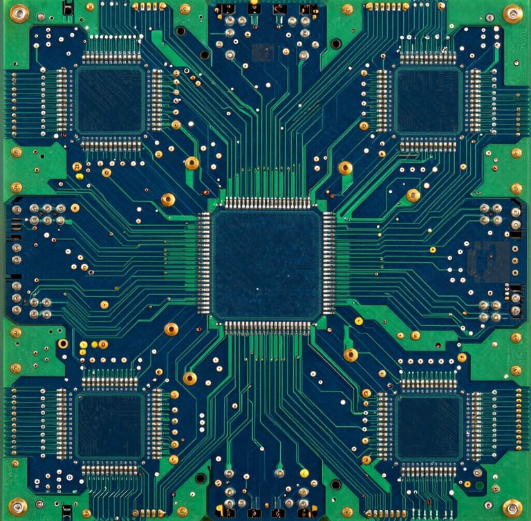
Extreme close-up macro photography of a multi-layer PCB, crisp trace paths illuminated with electric blue backlighting, sharp focus, 50mm lens, cool studio lighting
ENGINEERING PHILOSOPHY

Deliberate layout, trace by trace

We reject generic autorouters. Every high-density trace is hand-routed to maintain absolute signal integrity, manage thermal dissipation, and guarantee first-spin success on complex multi-layer boards.

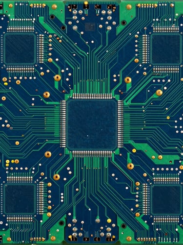
Overhead flat-lay shot of a dense, complex green and blue printed circuit board, highlighting gold-plated solder pads and high-density interconnect lines, sharp technical focus
THE DIRECT BRIDGE

From schematic to physical reality

A beautiful schematic is only the beginning. Our veteran engineers design layouts with deep awareness of fabrication limits, translating complex electrical concepts into high-yield physical hardware that scales seamlessly.

We optimize stackups, manage impedance matching, and design for strict physical and thermal constraints, ensuring your high-speed digital or RF boards perform flawlessly in volume production.

OUR COMMITMENT

We place every single trace manually to guarantee signal integrity.

By prioritizing manual routing over automated shortcuts, we eliminate crosstalk, manage thermal dissipation, and ensure your high-density interconnect hardware passes rigorous EMI testing on the very first spin.

Ready for first-spin success?

Send us your schematics and stackup requirements today. Our engineering team will return an ultra-precise layout optimized for immediate manufacturing.